


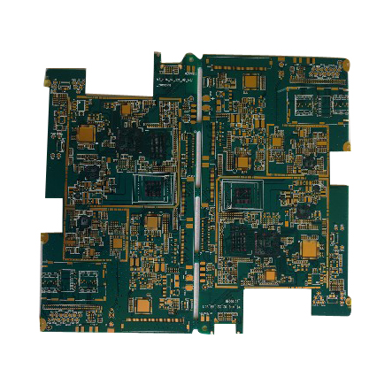

6-layer circuit board
Number of floors: 6 Thickness: 1.00±0.100mm Minimum aperture: through hole: 0.30mm, blind hole: 0.1mm Buried hole: 0.25mm Line width spacing: 0.064 mm/0.094 mm. Surface treatment: Ni-Au deposit +OSP
Parameters
Number of floors: 6
Thickness: 1.00±0.100mm
Minimum aperture: through hole: 0.30mm,
blind hole: 0.1mm
Buried hole: 0.25mm
Line width spacing: 0.064 mm/0.094 mm.
Surface treatment: Ni-Au deposit +OSP
Process
1阶HDI
机械埋孔激光盲孔技术
树脂塞孔技术
Application
消费数码


 复制产品链接
 长按图片保存/分享