


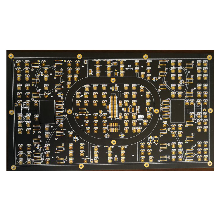

8 layer circuit board
Number of floors: 8 Thickness: 2.00±0.15mm Minimum aperture: blind hole: 0.10mm, buried hole: 0.225mm Line width spacing: 0.102mm/0.101mm Surface treatment: depositing nickel and gold.
Parameters
Number of floors: 8
Thickness: 2.00±0.15mm Minimum
aperture: blind hole: 0.10mm,
buried hole: 0.225mm
Line width spacing: 0.102mm/0.101mm
Surface treatment: depositing nickel and gold.
Process
含叠孔盲孔+埋孔的2阶HDI
3次层压,PP填胶技术,树脂塞孔技术
成型尺寸公差+0/-0.10mm
高密集焊盘

Application
LED显示


 复制产品链接
 长按图片保存/分享