


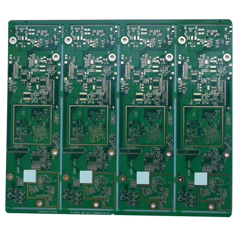

12 layer circuit board
Number of floors: 12 Thickness: 1.20±0.12mm Minimum aperture: through hole: 0.25mm blind hole: 0.10mm Buried hole: 0.225mm Line width and line spacing: 0.061mm/0.094mm Surface treatment: depositing nickel and gold.
Parameters
Number of floors: 12
Thickness: 1.20±0.12mm
Minimum aperture: through
hole: 0.25mm
blind hole: 0.10mm
Buried hole: 0.225mm
Line width and line spacing: 0.061mm/0.094mm
Surface treatment: depositing nickel and gold.
Process
3阶HDI,4次层压及层间对位技术
机械埋孔+激光盲孔+树脂塞孔技术
电镀填孔技术
PAD到线间距0.064mm,盲孔有叠孔和错孔
Application
交互智能平板


 复制产品链接
 长按图片保存/分享